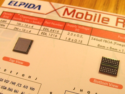
Elpida meldt op haar website een doorbraak op het gebied van DDR-II. Men heeft een 64MB DDR-II chip gebouwd die een gigabit per seconde per pin kan doorvoeren. Dit is 7,5 keer zo snel als PC133 en 75% sneller dan DDR266. De chip had hiervoor een read/write cycle van minder dan 4ns en een access time van minder dan 8ns nodig, en moest vanwege het lage voltage zeer zuivere signalen af kunnen geven. Hiervoor is een extreem nauwkeurig kloksysteem ontwikkeld met een afwijking van minder dan 30 biljoenste seconde. De chip is hierdoor meer dan goed genoeg om te voldoen aan de gespecificeerde 533Mbps van DDR-II. Het bedrijf heeft er zelfs vertrouwen in dat de technologie gebruikt kan worden voor toekomstige DDR-III chips:
- Output Skew Control: to eliminate output skew caused by device characteristics, operation voltage, and temperature fluctuations, Elpida has developed:
- Low-power, high-resolution digital delay-locked-loop (DLL): Includes clock regeneration circuits to align the output data timing with the input clocking at 1.6 V operation or lower.
- Output buffer circuit: Adjusts the output buffer impedance while maintaining the slew rate of output signals. These new circuits can reduce the output skew to as low as 10 ps, enabling the component to realize its potential of 1 Gbps.
- Reduced Cycle and Access Time: To reduce read/write cycle time and access time, Elpida has designed a new architecture that includes:
- Low-impedance hierarchical I/O architecture that calls for routing divided I/O lines over the memory cells with no tightening of the wiring pitch. This reduces the load of I/O lines by 50% and enables a 2.2 ns reduction of the read/write cycle time.
- Distributed data transfer scheme prioritized by ordered data. The new architecture achieves 4 ns read/write cycle time, which is a 45% reduction in access time to accommodate the 1 Gbps data rate of the DDR-II architecture.
Wederom danken we jamf voor de submit.

:strip_exif()/i/1032192616.jpg?f=fpa)
:strip_exif()/u/16793/metal.gif?f=community)
/u/12038/crop69547035714ff_cropped.png?f=community)
:strip_exif()/u/818/we33ee45.gif?f=community)
:strip_exif()/u/38491/klus.gif?f=community)
:strip_exif()/u/25674/medeadhead6060.gif?f=community)
:strip_exif()/u/7013/spunky_main.gif?f=community)
:strip_icc():strip_exif()/u/9740/crop59a4480aa191a_cropped.jpeg?f=community)
:strip_icc():strip_exif()/u/30282/1029_60x60.jpg?f=community)
:strip_exif()/u/45137/1blue1.gif?f=community)
:strip_exif()/u/29605/Q4O.gif?f=community)
:strip_exif()/u/35573/0sm.gif?f=community)
:strip_icc():strip_exif()/u/12152/butters.jpg?f=community)
/u/13698/Balance_60.png?f=community)
:strip_icc():strip_exif()/u/37767/crop6580b1fac90ae_cropped.jpg?f=community)