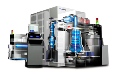
PcDealer schrijft: "ASM Lithography uit Veldhoven (30 minuten van mijn huis ![]() ) heeft via een press release laten weten dat zij de PAS 5500/1100TM op de markt brengen. Dit machientje van boven de 100 miljoen US dollar maakt het fabrikanten mogelijk om in hoog tempo IC-tjes met 100 nanometer connecties te bakken.":
) heeft via een press release laten weten dat zij de PAS 5500/1100TM op de markt brengen. Dit machientje van boven de 100 miljoen US dollar maakt het fabrikanten mogelijk om in hoog tempo IC-tjes met 100 nanometer connecties te bakken.":
VELDHOVEN, The Netherlands, November 7, 2000 -- ASML today introduced its newest 193nm Step & Scan lithography tool for high-volume production of semiconductor devices at the 100nm technology node. The PAS 5500/1100TM system provides the highest value of ownership for leading-edge IC makers by combining a 0.75 numerical aperture (NA) lens, improved leveling performance and industry-leading overlay with an exposure capacity exceeding 90 200mm wafers per hour at a dose of 20 mJ/cm2.
ASML entered the 193nm lithography equipment market two years ago when it introduced its PAS 5500/900TM tool, the semiconductor industry's first wide-field, 193nm Step & Scan system. Leveraging the process experience gained from its predecessor, the PAS 5500/1100 makes the next productivity leap in 193nm volume manufacturing.
The PAS 5500/1100 Step & Scan tool utilizes Carl Zeiss’ new StarlithTM 1100 lens, whose 0.75 NA equals the industry's largest. High-quality optical materials and coatings result in high transmission of 193nm-wavelength light. The illumination source is a 2 kHz, 10 W laser with a bandwidth of 0.35 pm.
The PAS 5500/1100 is ASML’s first lithography system to feature reticle alignment at actinic (blue) wavelength, using the 193nm exposure light. The PAS 5500/1100 also includes ASML’s patented ATHENATM wafer alignment system, enabling the tool to deliver industry-leading overlay accuracy. In addition, the wafer-leveling system has been substantially enhanced over previous PAS 5500 models to ensure depth-of-focus process latitude.
"Our new PAS 5500/1100 product supports the imaging requirements of the world’s leading-edge IC makers as they migrate to 100nm volume production," said Martin van den Brink, executive vice president of marketing and technology at ASML. "This newest addition to our product portfolio is one of the most advanced 193nm lithography tools available today, providing tighter resolution, better process overlay and higher throughput than any other system currently available on the global market."
Initial shipments of the PAS 5500/1100 will begin in March 2001.
 |
