Dan's Data heeft een review gepost van de inmiddels welbekende Asus A7V Socket A moederplank met VIA KT133 chipset, 5xPCI, 1xISA, AGP Pro en 3 keer DIMM. Het plankje dat door Dan werd getest is de oude revisie zonder multiplier dipswitch, waardoor er zonder zelfbouwacties (Dan legt hiervoor een sympathiek linkje met ons eigen Tweakers.net) alleen via de FSB overgeklokt kan worden:
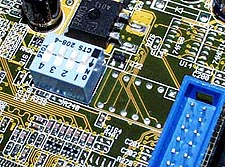
See the blank space to the right of the DIP switch block? Those 12 solder pads can accept another six switch block, which you can use to set the multiplier, provided you've got an unlocked processor.A bit of fiddling with my multimeter revealed that all of the top pads are connected to ground, but what the connections for the bottom pads are is more than I can be bothered figuring out.
ASUS are, at this moment, cranking out the manuals for the later A7V versions, which'll have switches in this location and mention of their settings in the documentation.
If you've got an original model A7V, like this one, and are vaguely handy with a soldering iron, you should only need to download the new manual. The 12 pads are plain solder-through holes to the other side of the circuit board, so you shouldn't need godlike soldering abilities to retrofit a switch block. You can get the switches from most decent electronics suppliers. In a pinch, you could just use wire links to make the settings.
  |
Verder wordt er in de review helaas weinig gezegd over de stabiliteit en busspeed overklokbaarheid van de Asus A7V.


/u/4153/crop5eb7889ee6872_cropped.png?f=community)
:strip_icc():strip_exif()/u/9434/b17_2.jpg?f=community)
:strip_exif()/u/1122/rrani.gif?f=community)