Intro
 Tweakers log, stardate 00200700, time 0255: After reports that the Duron and Thunderbird multiplier would after all be locked by AMD, a race against the clock started. All over the world overclockers and other fanatics worked frantically to find a solution to break this multiplier lock as quickly as possible.
Tweakers.net naturally couldn't be left out, so in very little time a mainboard was arranged and a processor bought. Tuesday afternoon at 14:00 hours Jasper, Floris, and myself were ready with the soldering iron, wires, jumpers, and soldering tin. Before us were a GigaByte GA-7ZM and a Duron 600.
On the following pages you can read about our adventures. Although the technology is occasionally a bit difficult, we have tried to keep it understandable for everyone. We have written this article in just a few hours under large time-pressure, so you may find a few rough edges here and there. We apologise for this in advance.
Some general information upfront
The Duron multiplier is set by two factors, FID and BP_FID (FID = Frequency ID). The signal from FID is sent from the CPU to the mainboard's northbridge. Then the northbridge sends a signal back to the CPU which actually sets the multiplier that the CPU is going to use. The trick is to modify the signal that is sent by the CPU to the northbridge to change the multiplier. The BP_FID pins send a signal directly to the CPU, which has to match the FID signal or the system won't boot.
Because BP_FID wasn't documentated in AMD's datasheets it was really hard to find the solution for the described problem. With quite a bit of help from Hiroji, who first found out about the undocumented BP_FID pins, and an informative Xoom site, who put us on the trail of the L1 bridges (among other things), a battleplan was made for attacking the problem.
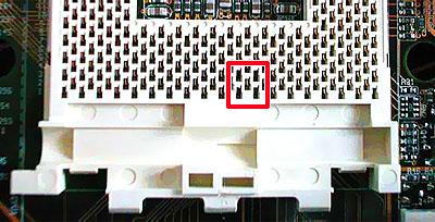
The Duron's multiplier was locked by laser-cutting 4 golden bridges (marked L1). By doing this the connection with the BP_FID pins is cut off, resulting in a signal inchangeable from the socket. Some retail Durons and Thunderbirds are locked this way, including ours. Most at this time still seem to be coming with the L1 bridges intact (we have had esxactly one other report of a locked processor to date). This picture (borrowed from uncle Tom) shows an unlocked Duron: the L1 bridges are still intact.
Further there are differences between mainboards. Some boards, like the Asus A7V, provide a possibility to change the mulitplier. The Gigabyte GA-7ZM that we used didn't have such a possibility.
Adding this together makes you end up with these four possible situations.
 Duron not locked + mainboard with multiplier tweaking onboard
Duron not locked + mainboard without multiplier tweaking
Duron locked + mainboard with multiplier tweaking
Duron locked + mainboard without multiplier tweaking
The most simple situation is the first one (duh!). In that case you only need to set some dipswitches and you're done. With the third option you will "only" need to alter the Duron itself, a modification that eventually proved to be quite simple. If you happen to already own a Socket A mainboard without multiplier tweaking options, you have some more work to do. You'll have to build a multiplier tweaking system yourself.
Our task was the hardest: we had to unlock the Duron and try to modify our mainboard in a way that we could actually control the multiplier. The exact way we did this is explained in the next pages.
Changing FID
The FID story is quite simple. The FID is a 4-bit signal. Usually, for every bit a connection is made from the CPU to the northbridge. The northbridge connects the signal to Vio through a resistor. If nothing else happens to it, the signal line is "high". Through the mainboard, the socket, a pin on the Duron and the CPU itself the signal finally reaches one side of the golden bridges on top of the CPU. The other side of the golden bridges are connected with 0V.
For every bit the rule is that if its corresponding golden bridge is open, the bit is positive (1). A closed bridge means the bit is negative (0). Now what we want to accomplish is that the cpu isn't going to set these bits, but we set them ourselves instead. The solution is very simple: we use a soldering iron to remove the corresponding pins in the socket, which disables the bridges. Next we solder a wire to a set of jumpers or dipswitches, which wil take over the function of the golden bridges.
You can see what we did in this schematic. On the left is the situation before the "treatment" and on the right you can see the situation after our soldering iron did its work.
Step one is to detach the CPU's pins of the mainboard. The easiest way is by removing the corresponding connectors from the socket. It takes some effort to open the socket, but with a little handyness and some persistence it can be done. Next you remove the connectors by heating the solder of the four pins under the mainboard so you can pull out the pins very easily. We advise that you practice first on an old mainboard or a cheap slotket-convertor. You don't want to wreck your brand-new mainboard of course. The final result looks like this:
Step two is to make the connection between the jumpers/dipswitches and the connection under your mainbord which corresponds with the connectors you have just removed from the socket. If you're a little handy with the soldering iron it is all quite easy to manage.
Changing BP_FID
BP-FID is actually easier, if your cpu isn't locked. BP-FID, like FID, consists of 4 bits, where FID and BP-FID should be equal, otherwise the cpu won't work (unless BP_FID is lower than FID, in which case the BP_FID setting is used for some inexplicable reason -- which conveniently explains Anand's results with being able to underclock but not overclock). So we also have to change BP-FID in order to change the multiplier.
Every signalline of the BP-FID is connected (through the golden bridges on the cpu and a resistor) to either approx. 2.0V or 0V. Also, they are connected via a second golden bridge to pins on the cpu which is described by AMD (very sneaky) in the datasheet as "Not Connected". Next, this signal goes to the cpu that uses it to check if the signal from the FID will be accepted.
In order to ignore the golden bridges of the cpu, follow these easy steps: You create a jumperblock, with wires in the middle that go to the "Not Connected" pins, and on each side you put 0V and ~2V. With these jumpers you can "override" the cpu adjustments.
(the Dutch text can be easily understood when you know that "naar" means "to" in English).
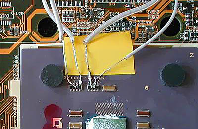
At this moment we presumed that the internal connection between the BP-FID pins on the cpu and the L3 and L4 bridges didn't exist anymore. The only solution was to make a connection around the cpu, by soldering 4 wires at the resistors (the 2 rectangular blocks).
And here comes the magic trick: The connection between L3, L4 and the BP-FID pins still exists, only, it runs via the L1 bridges! Because AMD took this connection away, the BP_FID pins are marked as "Not Connected" in the datasheets. By closing the L1 bridges you can get full control over BP_FID through the mainboard, and that what it's all about!
With a mainboard that already has this function on-board, you are ready. If you don't have this then you still must make it yourself, like at FID, with the advantage that you don't have to pull connectors out of the socket. You find more about this later in the review.
Motherboard modifications
I'm going to keep this part of the article rather technical, if you don't understand it, it's better to ask someone with more experience in soldering to do it for you. So what should be done, without all the theory?
When you assemble the following part on a piece of experiment board (a board full of holes), then all you have to do is to connect a few wires. The first 4 jumpers are for BP_FID, the second set of 4 jumpers are for FID, and the third set is for VID, but you probably won't need to use this because most mainboards already come with voltage-tweaking capability.
After assembling this you connect a bunch of small wires on that middle/upper row of contacts. Then it gets slightly hard: You have to de-assemble the socket so that the cap comes off, and then you can solder the following pins out of the socket: W1, W3, Y1 and Y3. If you also want to install voltage-tweaking, repeat this for pins L1, L3, L5, L7 and J7.
The wires that come from your jumperboard should be connected, from left to right, on the following points under the socket on the mainboard: AL25, AN25, AL27 and AN27, then Y3, Y1, W3 and W1, and if you wish to install voltage tweaking also on J7, L7, L5, L3 and L1. After that you have to connect the 0V and 3.3V connectors of the jumperboard on the ATX power supply connector, and you're ready!
The table with settings for both BP_FID and FID is as follows
All these adventures result in this situation:
1 = BP_FID. After connecting the L1 bridge this cable is connected under the mainboard.
2 = FID. This cable is connected to 4 pins under the socket.
3 = VID: Voltage adjustments. This also should go through the backside of the socket.
4 = the power supply of the jumperboard. For this 3.3 Volt should be taken of the ATX-Power supply.
Unlocking a locked processor
What if you, just like us, get a locked Duron, where the BF_FID pins are not connected to the die itself?
The guy from this Xoom page found that the golden bridges at L1 had to be involved. He found out that he could lock his Duron by cutting those bridges. We looked at our CPU and indeed, the bridges were cut while all Durons we have seen up till now had their L1 bridges closed. Don't worry, we can close those bridges again and thereby unlock the Duron.
At the local hardwarestore we bought some Bison Electro Kit. This is a special sort of glue with silver parts in it so it conducts electricity. The stuff is sold to fix VCR's etc.
With a needle we put a very little bit of this glue on the L1 bridges. Now the BP_FID pins are reconnected and we can change the multiplier on every mainboard with onboard multiplier tweaking. The Gigabyte mainboard we used has onboard multiplier tweaking too (after we modified it, of course), so we can change the multiplier.
What we did can be seen on the picture below.
After the mainboard treatment the bottom of the board looks like this: BP_FID is now connected to the pins which go through L1 to L3 and L4.
Final thoughts
If this is the only locking method AMD has in mind (removing the L1 connections), then there is still some good news for tweakers. It seems that it's very simple and reasonably inexpensive to reconnect these connections, and thereby fix the lock for the processor. Again: the only thing you'll have to do to unlock the Duron, is to reconnect the L1 bridges with a conductive glue or ink or something like that. If the bridges are already connected, your Duron isn't locked at all! This should also work with SocketA Thunderbird Athlons.
If you have a mainboard that already has jumpers or dipswitches to change the multiplier, tweaking the AMD Duron is very simple. If your mainboard doesn't have it, don't panic. You can make it yourself, as you can read in the article. It takes more time and energy, a stable hand and a lot of courage, but it can be done!
Our 600Mhz Duron is totally stable at 900Mhz, a 50% increase of the stock speed! Beyond that speed, heat is a very big problem. At 950Mhz the system needs watercooling with ice in the reservoir to be stable and at 1 Ghz it won't even boot Windows. Even idling in DOS kills it within 15 minutes.
In the forthcoming period we'll try to get the AMD Duron stable at 1 Ghz with the help of watercooling and/or peltiers. Even if AMD decides to remove the internal traces to the BP_FID (I wonder how they want to do that without redesigning the whole CPU, but ok) you can work that out. In that case, you have to make the connection outside the CPU, like we did before we found out that L1 was involved.
The End
The last days have been quite intense for the three of us (Jasper, Floris and Daniël). We tried very hard to make a review of a fully locked Duron, which can be overclocked easily. Furthermore, we were trying to be one of the first sites to write such an article.
The forthcoming days will be spent on finetuning the Duron and the review, so this story isn't over yet. New developments will be announced in the .plan updates. That will only be in Dutch however, unless we have some very important news to share of course  .
.
All that's left to say is a big thanx to Paul Hubert for giving us one of his Gigabyte mainboards for our tweaking adventures. And of course a big thanx to Jan Borger, E-Techz and troje for helping us out with translating this article!


:strip_icc():strip_exif()/u/1929/Lifeforms60x60.jpg?f=community)
:strip_icc():strip_exif()/u/1740/shark.jpg?f=community)
:strip_icc():strip_exif()/u/21/crop69f04ee6196b5_cropped.jpg?f=community)
:strip_icc():strip_exif()/u/7414/crop5fd76399bcfd7.jpeg?f=community)